ndia Advances in AI Chip Packaging with Paras and BroadPak
India's semiconductor industry takes a major step as Paras Semiconductors partners with BroadPak to explore advanced chip packaging, chiplet integration and technologies powering future AI hardware.
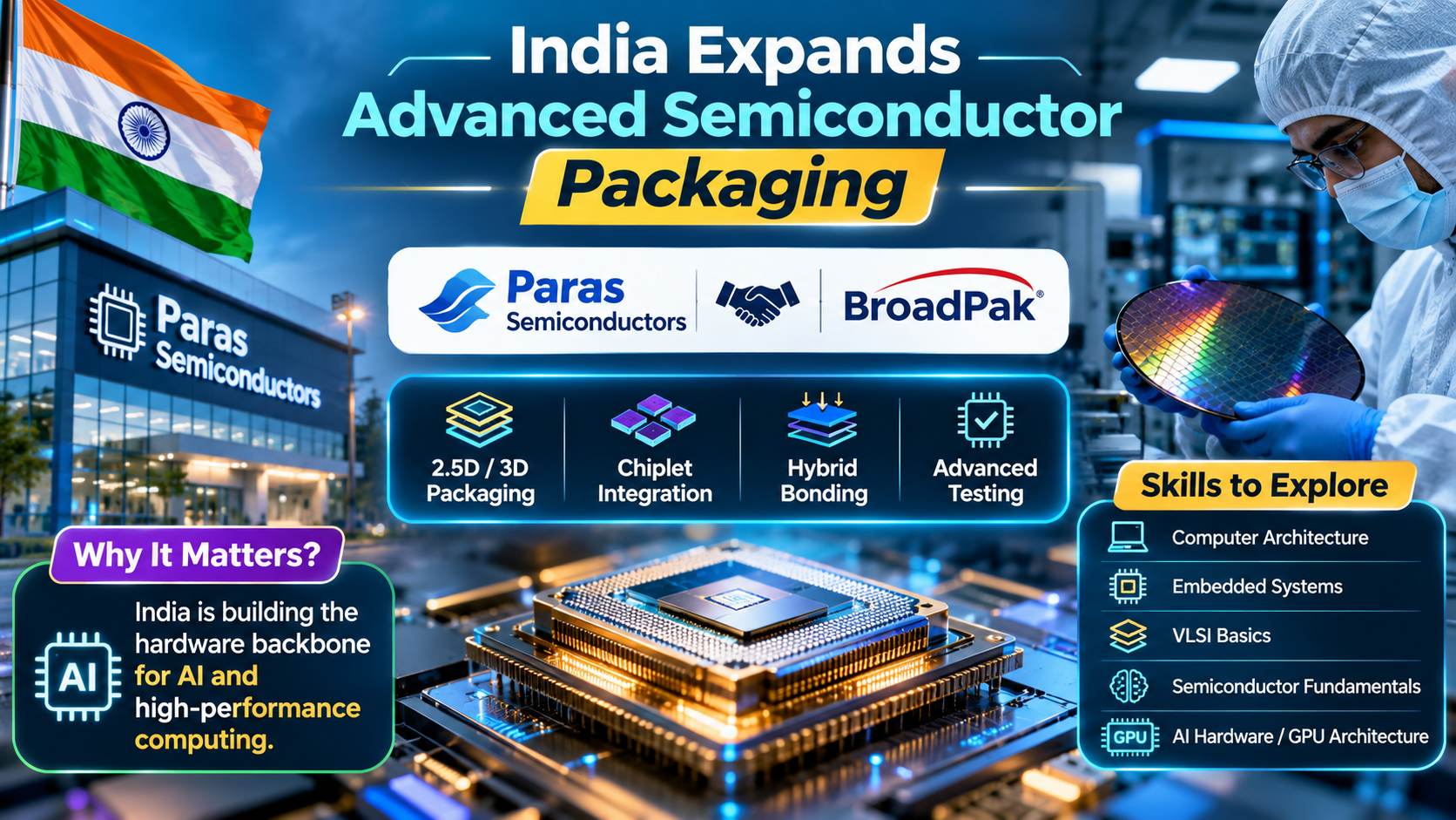
India's Semiconductor Industry Enters a New Phase: Paras Semiconductors Partners with BroadPak
Technology News · India · November 2026 · Approximately 7–9 minutes
The full news article
India Moves Towards Advanced Semiconductor Packaging
India is taking another step towards strengthening its semiconductor industry. Paras Semiconductors, a subsidiary of Paras Defence & Space Technologies, has announced a strategic technology partnership with US-based BroadPak Corporation to develop advanced semiconductor packaging capabilities in India.
The announcement, made on November 6, 2026, is important because the global technology industry is increasingly demanding powerful, energy-efficient chips for artificial intelligence, high-performance computing, cloud infrastructure and modern data centres.
The collaboration aims to establish an advanced heterogeneous integration and 3D packaging facility in India. It will focus on technologies such as 2.5D and 3D packaging, chiplet integration, hybrid bonding, wafer-level packaging, co-packaged optics and advanced semiconductor testing.
This development highlights an important change in the semiconductor industry: building a powerful processor is no longer just about manufacturing a smaller chip. How different components are connected, packaged and integrated is becoming equally important.
The Economic Times+1
1. What exactly happened?
Paras Semiconductors has joined hands with BroadPak Corporation to combine Indian manufacturing ambitions with specialised semiconductor packaging expertise.
Paras Semiconductors will work towards establishing advanced packaging manufacturing capabilities in India, while BroadPak will contribute technology expertise, design and manufacturing intellectual property, process knowledge and integration capabilities.
The proposed collaboration will support the development of packaging solutions for artificial intelligence, high-performance computing, networking, data centres and strategic electronics.
One of the important objectives is to build an advanced OSAT facility.
OSAT stands for Outsourced Semiconductor Assembly and Test. These facilities handle important stages after a semiconductor wafer has been manufactured. Individual chips are assembled, packaged, connected and tested before being used in electronic products.
The proposed facility is expected to develop capabilities across several advanced packaging technologies rather than concentrating only on conventional chip assembly.
According to additional reporting by ET Manufacturing, the proposed project is planned for the Ujjain–Indore corridor in Madhya Pradesh, with a reported investment of approximately ₹6,200 crore. Commercial production is targeted for the fourth quarter of 2028. These are project plans, not completed manufacturing achievements.
2. Why is advanced semiconductor packaging important?
To understand this development, imagine building a powerful computer.
A computer needs a processor, memory, communication components and other electronic parts. These components must communicate quickly and work together efficiently.
A semiconductor chip performs calculations and processes information. However, a modern AI system requires much more than a single chip.
It may need:
Powerful processors and GPUs.
High-bandwidth memory.
High-speed communication connections.
Efficient power management.
Advanced cooling and thermal management.
Advanced packaging brings multiple semiconductor components together into a compact, integrated system.
This can improve performance, reduce communication delays, increase bandwidth and help manage power consumption.
For AI systems, these improvements are especially important because large AI models process enormous amounts of information.
Without efficient communication between processors and memory, even a powerful chip can become limited by data-transfer bottlenecks.
That is why semiconductor packaging has become a critical part of modern AI infrastructure.
3. Four major technologies involved in the partnership
A. 2.5D Semiconductor Packaging
In traditional chip designs, components are often placed separately. In 2.5D packaging, multiple chip components are placed close together on a common interposer or advanced substrate.
This allows processors and memory components to communicate through high-density connections.
Why it matters:
Faster communication between components.
Higher memory bandwidth.
Better integration of multiple chips.
Improved performance for AI accelerators.
This technology is particularly useful for high-performance computing systems.
B. 3D Semiconductor Packaging
3D packaging takes integration further by stacking semiconductor dies vertically.
Instead of spreading every component across a flat surface, multiple layers can be connected vertically.
Benefits include:
Higher component density.
Shorter communication paths.
Compact chip designs.
Potential improvements in energy efficiency.
This approach is important for advanced memory systems and next-generation computing hardware.
C. Chiplet Integration
Effects of Poor Workload Partitioning on System Performance for Chiplet-Based Systems[v2] | Preprints.org
A chiplet is a smaller semiconductor component designed to perform a particular function.
Instead of manufacturing one enormous processor containing everything, engineers can combine several smaller chiplets into a single package.
For example:
One chiplet can handle computing.
Another can manage memory connections.
Another can handle input and output.
Additional chiplets can provide specialised functions.
This modular approach can improve design flexibility and allow companies to combine different technologies.
It is becoming increasingly important in advanced processors and AI hardware.
D. Hybrid Bonding
Hybrid bonding is an advanced method of connecting semiconductor layers using extremely fine-pitch electrical and physical connections.
It can enable dense connections between stacked chips and support advanced 3D integration.
Its potential benefits include:
Higher interconnection density.
Shorter electrical connections.
Better integration of memory and processors.
Improved system-level performance.
These technologies are closely connected to the future of AI accelerators and high-performance computing.
BroadPak+1
4. What role will BroadPak play?
BroadPak Corporation is a US-based semiconductor technology company headquartered in San Jose, California.
Its expertise includes advanced semiconductor packaging, heterogeneous integration, chiplet-based architectures, high-speed interconnections, thermal management and co-packaged optics.
Under this partnership, BroadPak is expected to support Paras Semiconductors through:
Technology transfer: Sharing specialised knowledge and processes required for advanced packaging.
Design expertise: Supporting the architecture and integration of complex semiconductor systems.
Manufacturing knowledge: Helping develop packaging and production processes.
Engineering support: Supporting the development and testing of advanced semiconductor solutions.
Skill development: Exploring collaborative training opportunities for Indian engineers.
The partnership is significant because advanced semiconductor manufacturing requires specialised equipment, engineering knowledge and years of technical experience. Access to international expertise could help Indian companies develop these capabilities faster.
The Economic Times+1
5. How will this help India's AI industry?
Artificial intelligence is growing rapidly across the world.
Companies are building increasingly powerful AI models that require enormous computing resources. Training and operating these models requires specialised processors, GPUs, memory systems and high-speed networking infrastructure.
This creates demand for advanced semiconductor packaging.
Consider some examples:
Industry | How advanced chips help |
|---|---|
Artificial Intelligence | Faster AI calculations |
Data centres | Efficient computing infrastructure |
Cloud computing | High-performance servers |
Automotive | Advanced electronic systems |
Defence | Strategic electronic equipment |
Telecommunications | High-speed networking |
India has been working to develop a stronger semiconductor ecosystem. This includes chip design, semiconductor manufacturing, assembly, testing and supporting industries.
The Paras–BroadPak partnership adds another development to this growing ecosystem.
It is particularly relevant because AI infrastructure is not limited to software companies. It also depends on the physical hardware that powers intelligent systems.
6. India's semiconductor ambitions: Why now?
India wants to become a more important participant in the global semiconductor supply chain.
For many years, semiconductor manufacturing and advanced packaging capabilities have been concentrated in a relatively small number of countries and specialised industrial regions.
As global demand for chips increases, countries are looking to diversify their supply chains and strengthen domestic manufacturing.
India has several potential advantages:
A large engineering talent pool.
Growing electronics and technology industries.
Government support for semiconductor development.
Increasing demand for domestic electronic products.
Opportunities in AI, automotive and telecommunications.
The NITI Aayog's 2026 semiconductor industry roadmap also identifies advanced packaging, OSAT capacity, chiplet assembly and 2.5D/3D integration as important areas for developing India's semiconductor capabilities.
NITI Aayog+1
This means advanced packaging is not just a single company's business opportunity. It is part of a broader effort to strengthen India's technology manufacturing ecosystem.
7. What is the expected investment and project timeline?
The proposed project has attracted attention because of its reported scale.
According to ET Manufacturing's November 6 report, the planned facility has several important targets:
Project detail | Reported plan |
|---|---|
Investment | Approximately ₹6,200 crore |
Location | Ujjain–Indore corridor, Madhya Pradesh |
Initial capacity | 10,000 wafers per month |
Construction target | First quarter of 2027 |
Commercial production target | Fourth quarter of 2028 |
Technology focus | Advanced packaging and OSAT |
The company has reportedly received approval from the Madhya Pradesh government and plans to seek support under India Semiconductor Mission 2.0. Central government incentives should not be treated as already approved.
The project is also expected to explore international customer opportunities.
It is important to understand that these figures represent proposed plans and targets. The actual progress will depend on construction, investment, equipment installation, technology readiness, customer demand and regulatory approvals.
8. What does this mean for engineering students in India?
This is one of the most interesting parts of the development.
Many engineering students focus mainly on programming languages, software development and artificial intelligence applications.
These skills are valuable, but the semiconductor industry offers another direction.
The growing demand for advanced chips creates opportunities across hardware and software engineering.
Here are some skills students can start learning.
1. Computer Architecture
Understand how processors, memory, registers, caches and instruction execution work.
Learn:
CPU architecture.
GPU architecture.
Memory hierarchy.
Parallel computing.
Processor design fundamentals.
2. VLSI Fundamentals
VLSI stands for Very Large Scale Integration.
It involves designing integrated circuits containing large numbers of transistors.
Learn:
Digital electronics.
Logic gates.
CMOS fundamentals.
Verilog or SystemVerilog.
Digital circuit design.
3. Embedded Systems
Embedded systems combine hardware and software to perform specific tasks.
Learn:
C and C++.
Microcontrollers.
Arduino.
ESP32.
Hardware communication protocols.
4. Semiconductor Fundamentals
Understand the basic science behind semiconductor devices.
Learn:
Diodes and transistors.
Semiconductor materials.
Integrated circuits.
Wafer manufacturing.
Chip fabrication and packaging.
5. AI Hardware and GPU Architecture
AI applications require specialised hardware.
Explore:
GPU computing.
Parallel processing.
CUDA fundamentals.
Memory bandwidth.
AI inference optimisation.
These skills can help students explore careers in semiconductor design, hardware development, testing, embedded systems and AI infrastructure.
9. Five practical projects students can build
Instead of only reading about semiconductors, students can develop small projects to understand the concepts.
Project | What you will learn |
|---|---|
CPU simulator | Processor architecture |
Digital logic simulator | Logic gates and circuits |
FPGA-based calculator | Digital hardware design |
Memory hierarchy simulator | Cache and memory performance |
GPU performance comparison | Parallel computing |
For CSE and AI/ML students, a particularly interesting project would be a CPU and GPU performance comparison dashboard.
You could create a Python application that compares processing time, memory usage and execution performance for different computational tasks.
This connects programming knowledge with computer architecture.
10. Career opportunities in the semiconductor industry
The semiconductor ecosystem includes many different engineering roles.
Some career paths worth exploring include:
VLSI Design Engineer
Semiconductor Test Engineer
Hardware Design Engineer
Embedded Systems Developer
Physical Design Engineer
Verification Engineer
Computer Architecture Engineer
AI Hardware Engineer
Semiconductor Process Engineer
Packaging and Reliability Engineer
Not every role requires the same degree or skill set. Some are more suitable for ECE and EEE graduates, while others are accessible to CSE students with the appropriate hardware, architecture or software specialisation.
For students interested in AI and machine learning, AI hardware, GPU computing, compiler optimisation and systems engineering are particularly relevant areas to investigate.
11. Challenges India must overcome
Although this partnership is promising, building a competitive semiconductor packaging industry will not happen overnight.
India will need to address several challenges.
High infrastructure costs: Advanced packaging facilities require specialised machinery, cleanroom environments and reliable utilities.
Technical expertise: Developing advanced packaging capabilities requires experienced engineers and specialised manufacturing knowledge.
Supply chain: Semiconductor packaging depends on advanced substrates, materials, equipment and specialised components.
Quality and reliability: Chips must undergo strict testing to ensure that they operate correctly under different conditions.
Global competition: Established semiconductor manufacturing countries already have significant experience, infrastructure and customer relationships.
Commercial execution: Announced partnerships and proposed facilities must translate into operational factories, reliable production and actual customer orders.
Successfully addressing these challenges will be important for India's long-term semiconductor ambitions.
12. What could happen next?
The next important developments to watch include:
Progress on the proposed facility in Madhya Pradesh.
Technology transfer and engineering collaboration between Paras and BroadPak.
Equipment installation and manufacturing readiness.
Customer partnerships in AI, networking and high-performance computing.
Recruitment and training of semiconductor engineers.
Commercial production against the announced project timeline.
These developments will help determine how quickly India can build advanced packaging capabilities.
Final thoughts: India's AI future needs hardware too
The Paras Semiconductors and BroadPak partnership highlights an important transformation in India's technology industry.
For years, India has been widely recognised for software development, IT services and engineering talent. Now, opportunities are expanding towards semiconductor manufacturing, advanced packaging and AI hardware.
The future of artificial intelligence will depend not only on better algorithms and larger AI models but also on powerful processors, efficient memory systems and advanced semiconductor technologies.
For engineering students, this is a good opportunity to explore beyond traditional programming.
Learning Python, C++, computer architecture, digital electronics, VLSI fundamentals and GPU computing can provide a stronger understanding of the complete technology ecosystem.
The bigger lesson is simple: AI needs software, but powerful AI also needs powerful hardware. India's semiconductor journey is becoming an important part of that future.
SEO and publishing details
Tags – Add these individually:
india semiconductorparas semiconductorsbroadpakadvanced packagingAI hardwarechiplet technologyVLSI2.5D packaging3D packagingsemiconductor industry
SEO keywords: India semiconductor industry, Paras Semiconductors BroadPak partnership, advanced semiconductor packaging, AI chip manufacturing India, chiplet integration, VLSI careers.
Suggested SEO excerpt:
India's semiconductor industry takes a major step with Paras Semiconductors and BroadPak partnering to develop advanced packaging technologies for AI chips, GPUs and high-performance computing.
Reading time: Approximately 7–9 minutes, depending on reading speed.
Publishing recommendation: Use the generated semiconductor infographic as your cover image and select the Hardware & Chips category.
Editorial note: This article distinguishes announced partnership plans from completed manufacturing achievements. Verify future project milestones before publishing updates.